DLL: Circuit Design, Layout and Post-Layout Verification
🚀 Overview
This project presents the complete implementation of a Delay-Locked Loop (DLL) in 22nm FDSOI technology, covering the full design flow from circuit design to layout implementation and post-layout verification.
The work includes:
- Circuit-level design and analysis
- Layout design using Cadence Virtuoso
- Physical verification (DRC/LVS)
- Post-layout simulation with parasitic extraction
The objective is to achieve accurate timing alignment, stable locking behavior, and minimal layout-induced degradation.
Keywords:
🧩 System Design
The DLL is composed of three main functional blocks:
- Sample Signal Generation
- Sample-and-Hold Circuit
- Voltage-Controlled Delay Line (VCDL)
Together, they form a first-order closed-loop system with strong stability and fast locking capability.
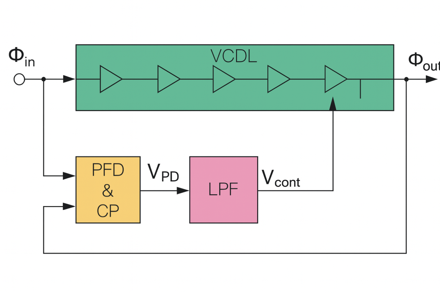
Block diagram of the Delay-Locked Loop (DLL)
⚙️ Core Modules
Sample Signal Generation
Pulse signals are generated using NAND and NOR logic:
- Rising edge → SAMPLE
- Falling edge → SAMPLE2
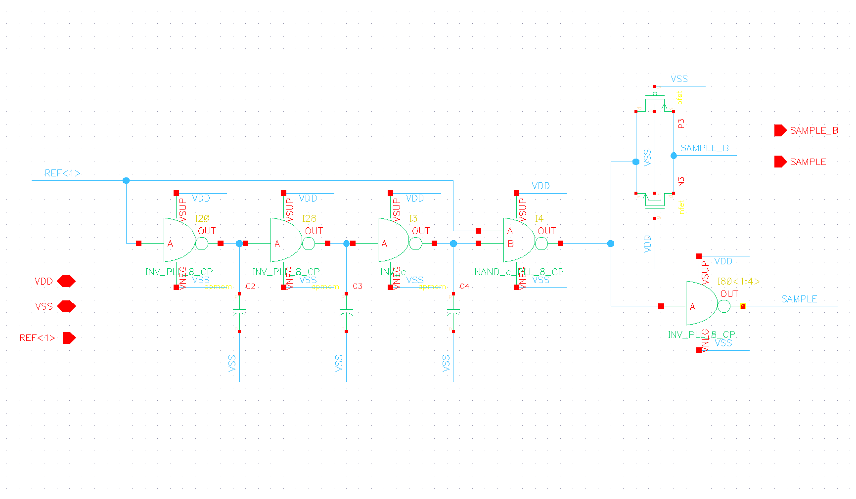
Sample signal generation using NAND gate
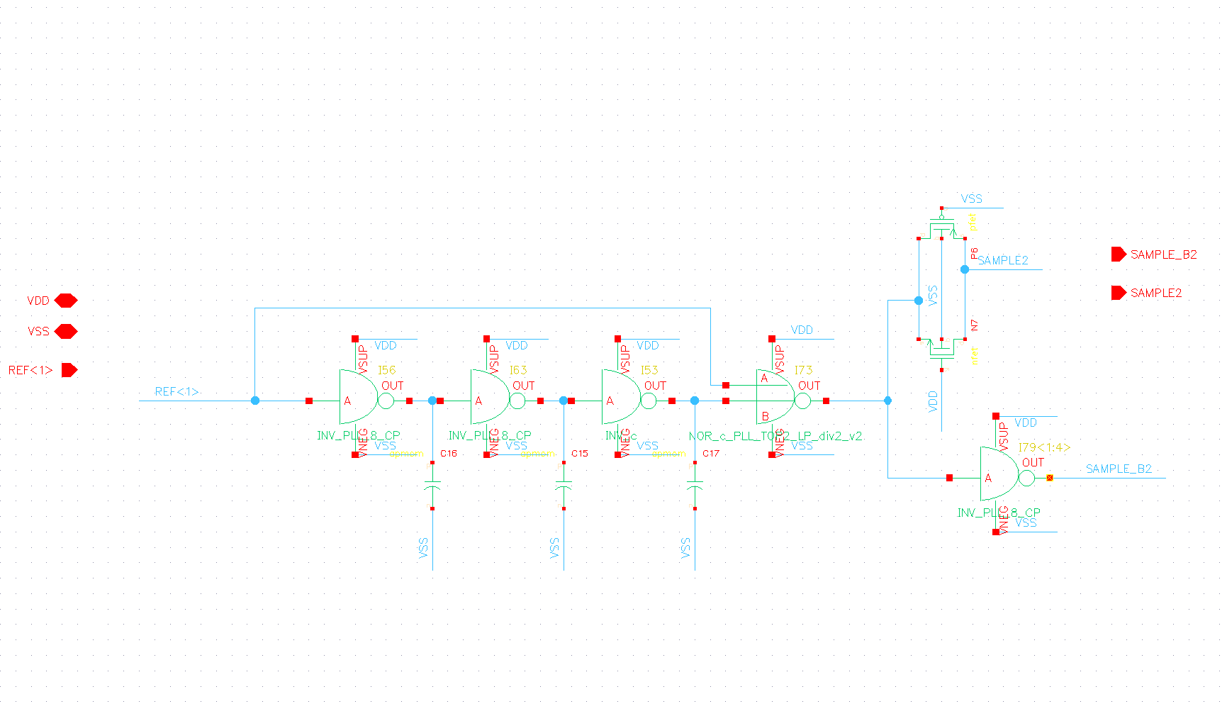
Sample signal generation using NOR gate
Sample-and-Hold
This block integrates:
- Phase detection
- Charge pump behavior
- Low-pass filtering
It produces control voltages:
- VCONT
- VCONT_N
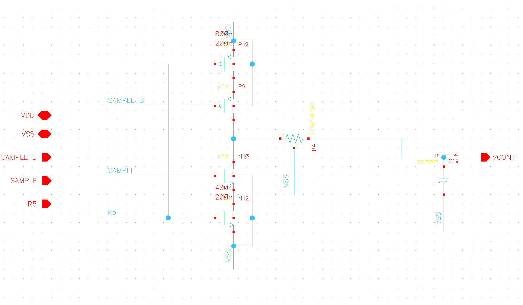
Sample-and-hold circuit structure
Voltage-Controlled Delay Line (VCDL)
The VCDL is the core component responsible for delay tuning:
- Differential architecture
- Monotonic delay control
- Stable phase adjustment
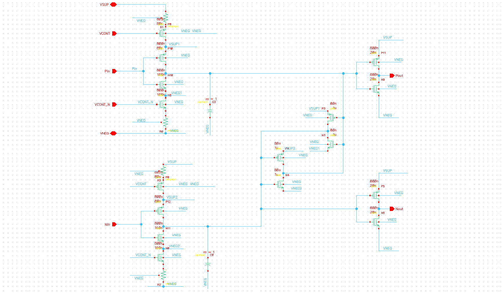
Differential VCDL cell structure
🧠 Working Principle
The DLL operates through iterative delay tuning:
- Detect phase difference
- Adjust control voltages
- Tune delay via VCDL
- Reach phase lock
At steady state:
- Each stage delay ≈ 1/8 T
- Total delay ≈ 1/2 T
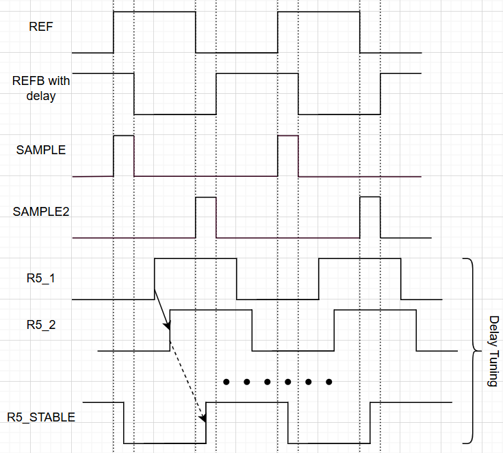
Waveform illustration of delay tuning process
🖥️ Layout Implementation
Key layout strategies include:
- Symmetrical transistor placement
- Parasitic minimization
- Area-efficient design
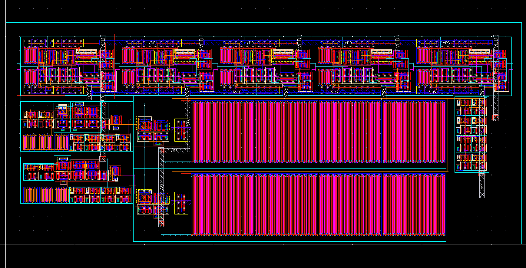
Final DLL layout with optimized symmetry and routing
📊 Results
Post-layout simulation confirms:
- Delay deviation: 0.5 ps – 3.5 ps
- Slightly faster locking than schematic
- Stable operation across all delay stages
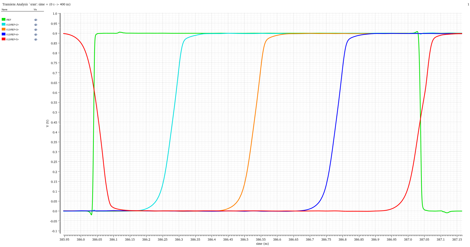
Post-layout simulation waveforms showing stable delay behavior
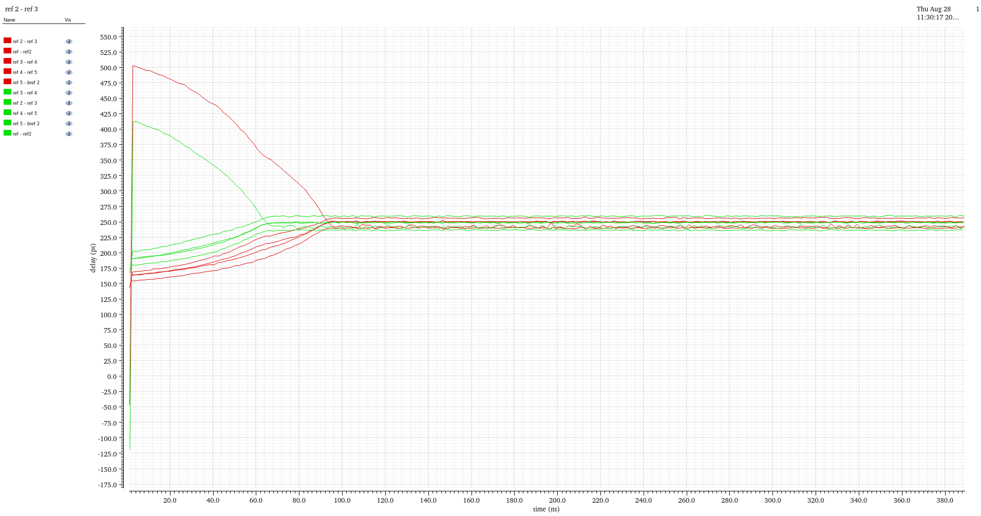
Comparison between schematic and post-layout delay results
🧾 Conclusion
This project demonstrates a complete mixed-signal IC design flow, from circuit-level understanding to layout implementation and post-layout verification.
The results confirm that:
- The DLL achieves accurate delay control with deviation within 0.5–3.5 ps
- Each stage introduces a delay of approximately 1/8T, achieving 1/2T total delay
- The system maintains stable locking behavior under post-layout conditions
Overall, the design validates the robustness and reliability of the DLL architecture for high-performance timing applications.
DLL:电路设计、版图实现与后仿验证
🚀 项目概述
本项目基于 22nm FDSOI 工艺,实现了一个 延迟锁定环(Delay-Locked Loop, DLL) 的完整设计流程,涵盖从电路设计到版图实现以及后仿验证。
主要工作包括:
- 电路级设计与分析
- 使用 Cadence Virtuoso 进行版图设计
- 物理验证(DRC / LVS)
- 寄生参数提取后的后仿真
项目目标是实现 精确的时钟对齐、稳定的锁定行为以及最小化版图寄生带来的性能影响。
关键词:
🧩 系统结构
DLL 由三个主要功能模块组成:
- 采样信号生成模块
- 采样保持电路
- 压控延迟线(VCDL)
整体构成一个 一阶闭环系统,具有良好的稳定性和快速锁定能力。
图 1.1:延迟锁定环(DLL)的系统框图
⚙️ 核心模块
采样信号生成
通过 NAND 和 NOR 逻辑门生成脉冲信号:
- 上升沿 → SAMPLE
- 下降沿 → SAMPLE2
图 3.1:基于 NAND 门的采样信号生成电路
图 3.2:基于 NOR 门的采样信号生成电路
采样保持模块
该模块集成了:
- 相位检测
- 电荷泵行为
- 低通滤波
用于生成控制电压:
- VCONT
- VCONT_N
图 3.5:采样保持电路结构
压控延迟线(VCDL)
VCDL 是实现延迟调节的核心模块:
- 差分结构
- 单调延迟调节特性
- 稳定的相位控制能力
图 3.9:差分结构的 VCDL 单元电路
🧠 工作原理
DLL 通过迭代调节延迟实现锁定:
- 检测相位差
- 调整控制电压
- 通过 VCDL 调节延迟
- 达到相位锁定
在稳态条件下:
- 每级延迟 ≈ 1/8 T
- 总延迟 ≈ 1/2 T
图 3.14:延迟调节过程的波形示意
🖥️ 版图实现
版图设计的关键策略包括:
- 器件对称布局
- 降低寄生效应
- 提高面积利用效率
图 3.17:优化后的 DLL 最终版图
📊 实验结果
后仿结果表明:
- 延迟误差:0.5 ps – 3.5 ps
- 锁定速度略快于原理图仿真
- 各级延迟稳定一致
图 4.1:后仿波形结果,展示稳定的延迟行为
图 4.2:原理图与后仿延迟结果对比
🧾 总结
本项目完成了从电路设计到版图实现再到后仿验证的完整混合信号 IC 设计流程。
实验结果表明:
- 延迟误差控制在 0.5–3.5 ps 范围内
- 每级延迟约为 1/8T,总延迟约为 1/2T
- 系统在后仿条件下能够稳定锁定
整体设计验证了该 DLL 结构在高性能时钟系统中的稳定性与可靠性。