Semi-Digital Phase-Locked Loop Design with Bandwidth Tracking
🚀 Overview
This project presents the design of a Semi-Digital Phase-Locked Loop (SDPLL) implemented in 22nm FDSOI technology.
The proposed architecture eliminates the need for a Time-to-Digital Converter (TDC) and introduces separate proportional and integral control paths to achieve high bandwidth and low jitter performance.
The design focuses on improving:
- Loop bandwidth stability across PVT conditions
- Locking robustness
- Phase noise and jitter performance
Keywords
🧩 Architecture
The SDPLL consists of the following main components:
- Phase Frequency Detector (PFD)
- Proportional Path
- Integral Path (generating multiple discrete control voltages)
- Voltage-Controlled Oscillator (VCO)
- Programmable Divider
- Initialization mechanism for VCO frequency to accelerate locking
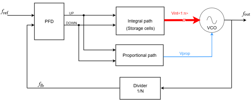
Proposed SDPLL architecture
Unlike conventional CPPLL, this design:
- Removes the loop filter resistor → no additional pole
- Eliminates the TDC → reduced complexity and power consumption
- Uses direct voltage injection → faster loop response
🔬 Key Design Techniques
Resistor-Free Proportional Path
- Eliminates thermal noise
- Reduces loop delay
- Enables higher loop bandwidth
Bandwidth Tracking Mechanism
To stabilize loop bandwidth across PVT conditions:
- The number of active Vint nodes is used as a PVT indicator
- The proportional path capacitance is dynamically adjusted accordingly
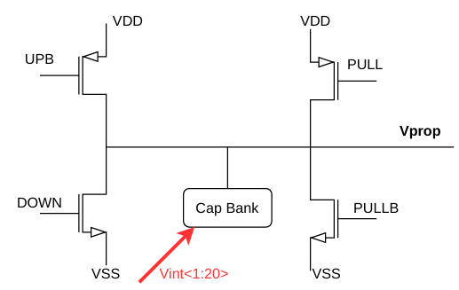
Bandwidth tracking mechanism based on Vint activation
Result:
fref / fBW ≈ 4–6
Divider Robustness Improvement
At slow corners, increased propagation delay may lead to instability in the divider.
Solution:
- Introduce an INITB-assisted initialization mechanism
- Ensure a valid startup state for reliable operation
VCO Headroom Optimization
Transistor sizing is optimized to improve:
- Maximum oscillation frequency
- Tuning range and headroom
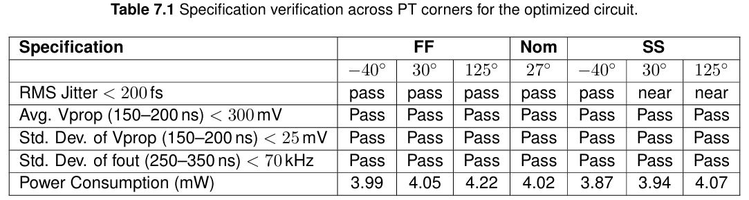
📊 Results
Performance summary:
- Output frequency: 5 GHz
- Reference frequency: 500 MHz
- RMS jitter: ~250 fs
- Power consumption: ~4 mW
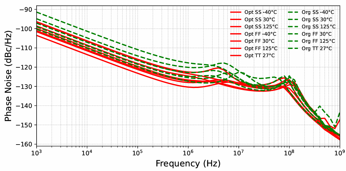
Phase noise comparison of the original and optimized PLL across corners.
🧾 Conclusion
This project demonstrates a TDC-free SDPLL architecture with:
- High loop bandwidth
- Low jitter performance
- Strong robustness across PVT conditions
The proposed bandwidth tracking mechanism effectively stabilizes loop behavior, making the design suitable for high-speed clock generation systems.
基于带宽自适应的半数字锁相环设计
🚀 项目概述
本项目设计并实现了一种基于 22nm FDSOI 工艺的半数字锁相环(SDPLL)。
该架构通过去除时间数字转换器(TDC),并引入分离的比例路径与积分路径,实现高带宽与低抖动性能。
本设计重点优化:
- 不同 PVT 条件下的环路带宽稳定性
- 系统锁定鲁棒性
- 相位噪声与抖动性能
关键词
🧩 系统架构
该 SDPLL 主要由以下模块组成:
- 相位频率检测器(PFD)
- 比例路径(Proportional Path)
- 积分路径(用于生成多个离散控制电压)
- 压控振荡器(VCO)
- 可编程分频器
- 初始化机制(用于预设 VCO 工作频率以加快锁定过程)
所提出的 SDPLL 系统架构
与传统 CPPLL 相比,本设计:
- 去除环路滤波电阻 → 无额外极点
- 无需 TDC → 降低复杂度与功耗
- 采用直接电压注入 → 提高环路响应速度
🔬 关键设计技术
无电阻比例路径
- 消除热噪声
- 减小环路延迟
- 提高环路带宽
带宽自适应机制
为实现不同 PVT 条件下的带宽稳定性:
- 利用激活的 Vint 节点数量作为 PVT 状态指示
- 动态调整比例路径电容
基于 Vint 激活状态的带宽自适应机制
结果:
fref / fBW ≈ 4–6
分频器鲁棒性优化
在慢角(SS)条件下,由于传播延迟增加,分频器可能出现不稳定。
解决方法:
- 引入基于 INITB 的初始化机制
- 确保系统启动时进入有效状态
VCO 余量优化
通过优化晶体管尺寸,提高:
- 最大振荡频率
- 调谐范围与频率余量
📊 实验结果
主要性能指标如下:
- 输出频率:5 GHz
- 参考频率:500 MHz
- RMS 抖动:约 250 fs
- 功耗:约 4 mW
原始与优化后 PLL 在不同工艺角下的相位噪声对比
🧾 总结
本项目提出了一种无需 TDC 的 SDPLL 架构,实现了:
- 高环路带宽
- 低抖动性能
- 良好的 PVT 鲁棒性
所提出的带宽自适应机制有效稳定了环路行为,使该设计适用于高速时钟生成系统。